Memory Mod: Difference between revisions
m (minor edits) |
m (minor edits) |
||
| Line 24: | Line 24: | ||
[[Image:Memory_Mod_Pic2.jpg|thumb|right|Fig.2. The AV7110 and SDRAM chips after the completed modifications to the board]] |
[[Image:Memory_Mod_Pic2.jpg|thumb|right|Fig.2. The AV7110 and SDRAM chips after the completed modifications to the board]] |
||
*'''Step1''': By gently pressing on the surface of the new/second SDRAM chip that you are adding to the board, ''carefully'' bend its pins such that they all, except for pin 18, can be made to connect 1:1 to first SDRAM chip's pins. Pin 18 |
*'''Step1''': By gently pressing on the surface of the new/second SDRAM chip that you are adding to the board, ''carefully'' bend its pins such that they all, except for pin 18, can be made to connect 1:1 to first SDRAM chip's pins. Pin 18, which is the /ChipSelect and is the 8th pin of the bottom line, starting from the right, will instead be connected to a thin wire soldered to the processor (see steps 4 and 5 of the modification process). To get a better idea of what this should look like, have a look at Fig.2 |
||
*'''Step2''': Attach |
*'''Step2''': Attach the second SDRAM chip onto the top of the existing one by soldering all the pins of the new chip (with the exception of pin 18) to the pins of the old one. Ensure that you have successfully connected the pins and that there are no short circuits. |
||
*'''Step3''': You will have to ''carefully'' scratch through the protective coating of the [[TI AV711x|AV7110]] until the protective coating is removed and a thin trace wire/line to the processor is exposed. Looking at the image in Fig.2, you will see that there are 6 round areas, the wire beneath the sixth with the small step is the one we need. Do not scratch deeply - if you see the copper shining, then that is enough/sufficient. If you scratch to deep, it will become impossible to solder onto that line, as is required in next step. |
*'''Step3''': You will have to ''carefully'' scratch through the protective coating of the [[TI AV711x|AV7110]] until the protective coating is removed and a thin trace wire/line to the processor is exposed. Looking at the image in Fig.2, you will see that there are 6 round areas, the wire beneath the sixth with the small step is the one we need. Do not scratch deeply - if you see the copper shining, then that is enough/sufficient. If you scratch to deep, it will become impossible to solder onto that line, as is required in next step. |
||
Revision as of 15:51, 10 January 2008
Memory Mod refers to upgrading a, so called, "full-featured" DVB card equipped with 2MByte SDRAM to 4MByte of SDRAM by means of placing another memory chip over an existing chip. The idea for this modification was introduced by Oliver Endriss.
The Idea
"Full-featured" DVB cards are equipped with a 2 MByte SDRAM chip. Using the Linux DVB drivers, OSD memory space is limited to approx. 80 KBytes. Therefore, it is not possible to have a full-screen, 256 color OSD when using VDR. However, the onboard AV7110/7111 MPEG-2 Decoder used by these cards is able to handle/address two 2MByte SDRAM chips. Doubling the amount of addressable memory onboard these cards would effectively resolve the limitation outlined above and, hence, users could gain a full-screen 256 color OSD in VDR. Additionally there would be more space for the video buffers. Given the obvious benefit, why not add the second one?
The Modification
The chip select for the second SDRAM chip is not available on the card's pcb itself, so the AV7110 processor and the memory chip have to be modified.
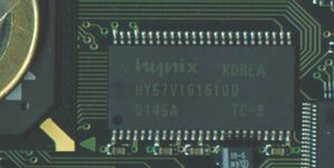
In Fig.1 at the side of the page, you can see both chips as they are found on the card prior to any modification; with the AV7110 processor on the left and the, completely visible, 2MByte SDRAM memory chip on the right. The area conveyed in the image is roughly equivalent to that of the face of a 1EURO coin.
The modification process is outlined as follows:
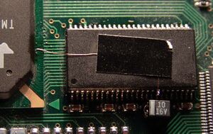
- Step1: By gently pressing on the surface of the new/second SDRAM chip that you are adding to the board, carefully bend its pins such that they all, except for pin 18, can be made to connect 1:1 to first SDRAM chip's pins. Pin 18, which is the /ChipSelect and is the 8th pin of the bottom line, starting from the right, will instead be connected to a thin wire soldered to the processor (see steps 4 and 5 of the modification process). To get a better idea of what this should look like, have a look at Fig.2
- Step2: Attach the second SDRAM chip onto the top of the existing one by soldering all the pins of the new chip (with the exception of pin 18) to the pins of the old one. Ensure that you have successfully connected the pins and that there are no short circuits.
- Step3: You will have to carefully scratch through the protective coating of the AV7110 until the protective coating is removed and a thin trace wire/line to the processor is exposed. Looking at the image in Fig.2, you will see that there are 6 round areas, the wire beneath the sixth with the small step is the one we need. Do not scratch deeply - if you see the copper shining, then that is enough/sufficient. If you scratch to deep, it will become impossible to solder onto that line, as is required in next step.
- Step4: Using a very thin wire of approx 0.1mm diameter, solder the wire to the processor's trace line that you have just exposed in Step 3.
- Step5: Connect/Solder the other end of the thin wire to pin 18 of the new SDRAM chip.
- Step6: Fix the thin wire and check the connection again
After these steps, a completed modification should look similar to the results shown in Fig.2. If all went well, and provided that a Firmware cognizant of the additional memory is made available to the card during system boot/startup, the processor should be able to use the full 4Mbytes now residing onboard the card.
List of suitable SDRAM chips
This list may be imcomplete. The AV71x needs 3.3Volt IO-Ports, therefore a 3.3Volt SDRAM in TSOPII packaging is needed. Some of that chips are on old graphics boards.
| Producer | Part Name | Informations |
| ESMT/EliteMT | M12L16161A-7T | homepage datasheet |
| EtronTech | EM636165TS-8 | homepage datasheet |
| Samsung | K4S161622E-TC80 | homepage datasheet |
| Goldstar | GM72V161621 |
Software Requirements
DVB driver with 4MB support and Firmware 261c or newer.
External Links
| [1] | vdrwiki:osdtest256-plugin | Plugin for testing of modded cards |
| [2] | vdrwiki:text2skin-plugin | plugin for loading of skins |
| [3] | http://www.rightchoiceelectronics.com/cr.html | Reference list with different ICs. Needed: 1Mx16 SDRAMs. |
| [4] | http://www.pcstats.com/ramfinder.cfm | RamFinder - Infos about RAM-ICs |
| [5] | http://www.wolfsoft.de | DVB Card Upgrade 2MB->4MB (~45 Euro) bzw. SDRAM (5,00+9,70)Euro |


